Two-dimensional materials hold tremendous promise in electronics, energy, and catalysis. In particular, high-mobility 2D semiconductors are expected to become next-generation channel materials for high-performance electronic devices.
However, defects and impurities at the gate dielectric–channel interface limit device performance, making a high-quality interface critical. Hexagonal boron nitride (hBN, or “white graphene”)—with its dangling-bond-free, atomically flat surface and excellent insulating properties—is an ideal interface material that minimizes interface damage and carrier scattering.
Achieving wafer-scale high-κ metal gate (HKMG) integration and high-performance 2D electronics requires overcoming challenges in hBN flatness, single crystallinity, large-area uniformity, and compatibility with semiconductor processes. Although CVD has enabled single-crystal hBN growth on metal substrates, controllable preparation of ultra-flat hBN wafers remains a major hurdle.
Recently,Chair Professor Ding Feng (Shenzhen University of Advanced Technology) and Professor Peng Hailin (Peking University) co-published a paper titled “Ultraflat single-crystal hexagonal boron nitride for wafer-scale integration of a 2D-compatible high-κ metal gate” inNature Materials. (Click “Read more” at the end for the full paper.) To address the challenge of controllable ultra-flat single-crystal hBN wafer preparation, Prof. Ding Feng’s team theoretically proposed a strategy of enhancing interfacial coupling (binding energy and friction), ensuring uniform domain orientation while suppressing wrinkles. In collaboration with Prof. Peng Hailin’s team at Peking University, they successfully achieved controllable growth of 4-inch ultra-flat monolayer single-crystal hBN wafers on Cu0.8Ni0.2(111)/sapphire substrates (as shown in Figure 1).
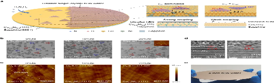
Figure 1.Schematic of the preparation of ultra-flat single-crystal hBN on CuNi(111)/sapphire substrate.
Theoretical calculations show that tuning Ni content in the Cu–Ni alloy modulates binding energy and friction between hBN and the substrate. As Ni content increases, binding energy rises, interlayer distance shortens, and friction increases, strengthening coupling and energetically favoring single-orientation domains.
Crucially, wrinkle formation on the growth substrate occurs in two steps: local hBN detachment forming small wrinkles, followed by sliding of detached hBN to enlarge wrinkles. Enhanced friction and binding energy suppress both steps (as shown in Figure 2), enabling ultra-flat single-crystal hBN wafers. Subsequently, uniform ultra-thin HfO₂ layers were deposited via ALD on 4-inch ultra-flat hBN wafers. The hBN/HfO₂ stack exhibited excellent dielectric performance, a low equivalent oxide thickness (EOT) of 0.52 nm, and low leakage current (2.36 × 10⁻⁶ A cm⁻²).
Guided by theoretical mechanisms,this work achieves controllable preparation of ultra-flat single-crystal hBN wafers and reveals that strong substrate–hBN interaction is key to ultra-flat single-crystal hBN films. This exemplifies Prof. Ding Feng’s long-standing philosophy of “theory-guided materials manufacturing.”
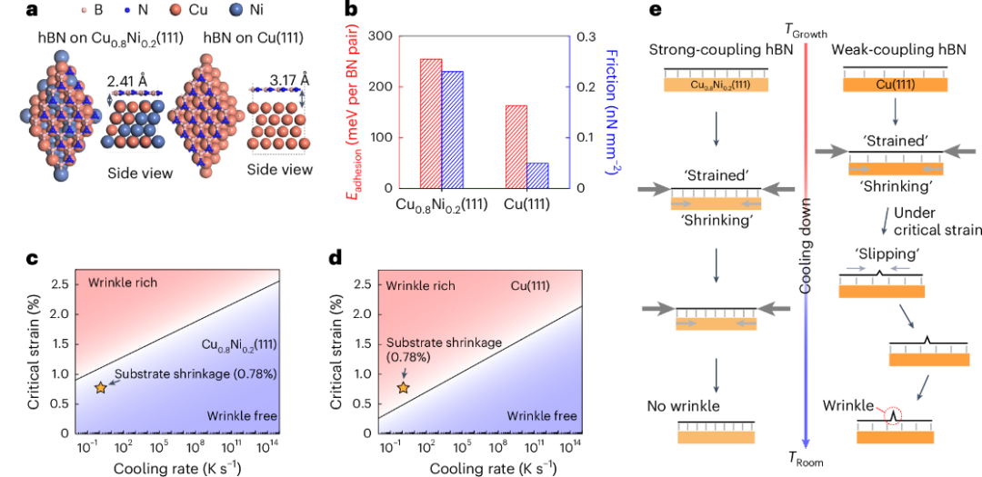
Figure 2. Wrinkle suppression mechanism of hBN on Cu0.8Ni0.2(111) substrate. (a) Atomic models of monolayer hBN on Cu0.8Ni0.2(111) (left) and Cu (111) (right) substrates. (b) Binding energy (red) and friction (blue) between hBN and Cu0.8Ni0.2(111) vs. Cu (111). (c–d) Critical stress for wrinkle formation as a function of cooling rate on Cu0.8Ni0.2(111) (c) and Cu (111) (d). (e) Schematic of wrinkle suppression on Cu0.8Ni0.2(111) (left) and wrinkle formation on Cu (111) (right) during cooling.
Shenzhen University of Advanced Technology and Peking University are co-corresponding affiliations. PhD students Yani Wang (College of Chemistry and Molecular Engineering, Peking University), postdoctoral researcher Chao Zhao (Shenzhen Institutes of Advanced Technology (SIAT), Chinese Academy of Sciences), PhD student Xin Gao (Institute for Interdisciplinary Research, Peking University), and Boya Postdoctoral Fellow Liming Zheng (Peking University) are co-first authors. Feng Ding (Shenzhen University of Advanced Technology) and Hailin Peng (Peking University) are corresponding authors.
Supported by NSFC, MOST, National Center for Beijing Molecular Sciences, Tencent Foundation, Peking University Boya Postdoctoral Fellowship, and the Molecular Materials and Nano-Fabrication Laboratory (MMNL) at Peking University.
 CN
CN